ATE PCB Design Services

Multilayer, High-Speed, and Controlled Impedance PCB Design for Semiconductor Test Platforms.

Request a ATE PCB Design Quote

Commitment to Excellence

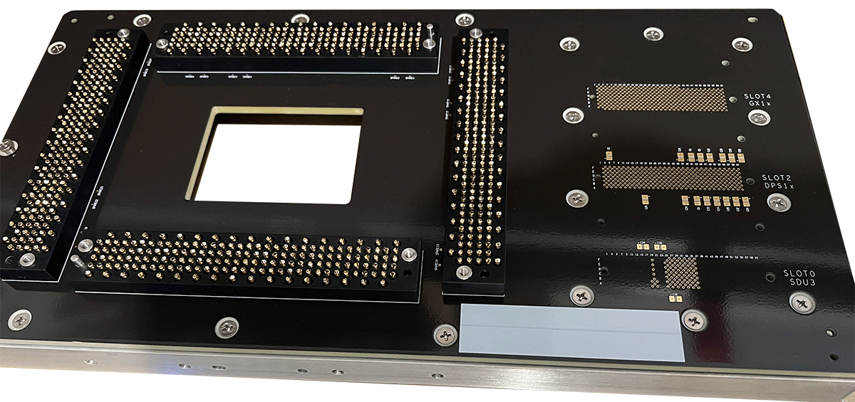
Finley Design has over three decades of experience designing Load Boards, Probe Cards, and DUT Interface Boards for semiconductor test environments. Our designs support mixed-signal, high-speed digital, and RF applications across leading tester platforms.

Our PCB Design Capabilities Include:

  • Single-sided, double-sided, and multi-layer boards
  • Rigid and flexible circuits
  • Controlled impedance routing
  • High-speed signal layout
  • Surface mount, through-hole, mixed technology
  • Power distribution planning
  • Design for manufacturability (DFM)
  • Design for testability (DFT)

Design Tools & Software

We utilize industry-standard PCB design tools to ensure compatibility with tester manufacturer specifications and downstream fabrication processes.

Cadence Design Systems

  • OrCAD Schematic Capture
  • Allegro PCB Editor
  • Allegro PCB Router

DownStream Technologies

  • CAM350

Autodesk

  • AutoCAD

Structured Design Process

Each project begins with a formal Design Input Specification. Our structured workflow ensures design accuracy, compliance with tester platform requirements, and readiness for manufacturing release.

Specification

The foundation of all of our designs is the Design Input Specification. After we have received all customer input regarding the project, we develop the Design Input. Throughout the design cycle this working document will be the guide for the Design Team, Design Review and our Production area. The Design Input outlines the specifications and requirements for the project.

Schematic

The Schematic provides the formulas for the design. The Schematic is one of the most important steps in the design as it will dictate how connections are made and determine the components needed. Once the schematic is complete and checked, a copy is provided to our customer for review and approval. Once approved, we are ready to start the Component Placement.

Component Placement

Another important step in the design process is the Component Placement. This can make a design and truly optimize your test performance. Our knowledge and experience matched with our intelligent tools allows us to work with our customers to create a superior design. Once approved, we are ready to begin to the Layout and make all of the connections.

Design Layout

The Design Layout is the step in the cycle when the connections are made. We also apply any special requirements such as length matching, differential pairs or any loop backs needed for your specific project. Once the layout is completed, a complete Design package is provided to our Design Coordinator for review.

Design Review

Using the Design Input, a thorough review is completed of the design package. We validate that the design meets the specifications of the project as well as ready to be fabricated and assembled. Once the review is complete, final design files are provided to the customer for review and approval. With the customers approval we are ready to Fabricate the project.